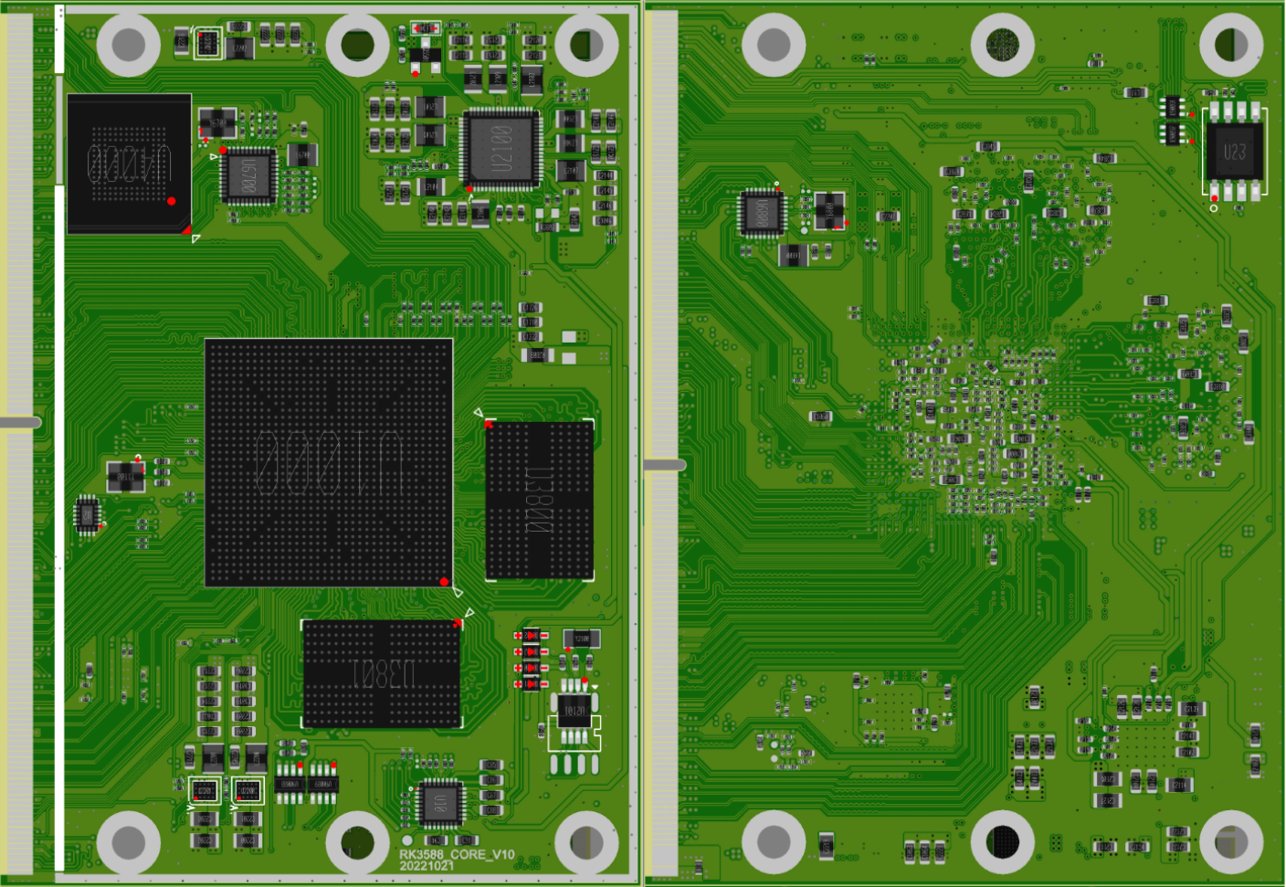
- CM5 is the smallest system core board based on RK3588. The core board provides external interfaces through metal fingers, and integrates 2X Gigabit Ethernet PHY, integrated audio CODEC, RTC and other functional modules inside the board. It can quickly help customers complete product planning, greatly reduce design barriers, and save development time.
- The following chapters provide a detailed introduction to the usage methods and precautions of each functional module, which can quickly help users complete product design. Maximize efficiency.
¶ Minimum system
¶ Power
- The core board uses a single power supply, with a power supply voltage range of 4.2V-5.0V, and a current of not less than 4A. It is strictly prohibited to have a voltage higher than 5.5V, which may cause damage to the power management chip.
- If the backplane power supply adopts a design of 12V to 4.8V, note that the soft start time of the power IC is not less than 2ms.
- The normal power of the machine is about 4W, and the network video is about 5W. However, if the system is heavily loaded or has high-power peripherals such as LCDs and mechanical hard disks connected, the power supply needs to be reassessed. Generally, it is recommended that the adapter power be not less than 12V/1.5A, which can meet most application scenarios.
Pin Number |
Pin Name |
Describe |
|---|---|---|
| B3 | VCC4V0_SYS | Main power input |
| B4 | VCC4V0_SYS | Main power input |
| B5 | VCC4V0_SYS | Main power input |
| B6 | VCC4V0_SYS | Main power input |
¶ Reset
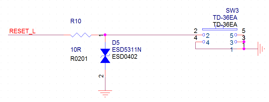
- The hardware reset of the CM5 is input through the Pin B7 (RESET_L) pin and must be controlled externally. The low level is effective. To ensure the stability and normal operation of the core board, the minimum reset time required is 100 24 MHz master clock cycles, that is, at least 4 us or more.
- Pin B7 (RESET_L) requires an additional 100nF capacitance to eliminate jitter on the reset signal, enhance anti-interference capabilities, and prevent abnormal system resets caused by false triggering.
- RESET_ The L network CM5 has pull-up processing internally, so there is no need to increase the pull-up resistance externally.
- To prevent damage caused by static electricity, it is recommended to reset the signal series resistance and increase ESD protection.
Pin Number |
Pin Name |
Describe |
|---|---|---|
| B7 | RESET_L | System reset signal |
¶ Usb otg port
- The DM DP corresponding to the TYPEC0 interface has the OTG function. As a device, it can download firmware from the computer to the machine and support ADB debugging. In HOST mode, it can be used to connect USB drives, mice, and other general-purpose USB devices. TYPEC1 can only be used as a HOST.
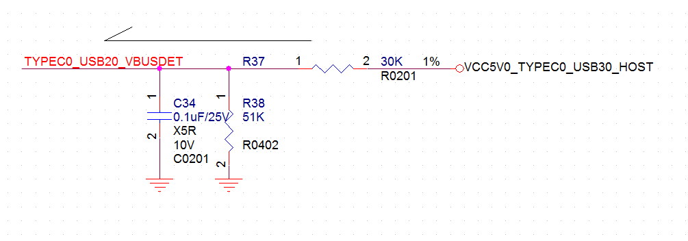
- The TYPEC0_USB20_VBUSDET signal must be led out, otherwise the machine cannot burn firmware normally. The 5V power supply of the USB interface is connected to the corresponding pins of the core board through a voltage divider resistor. Ensure that the voltage of this pin does not exceed 3.3V. If using a standard typec interface design, it is recommended to add a 3.0V TVS.
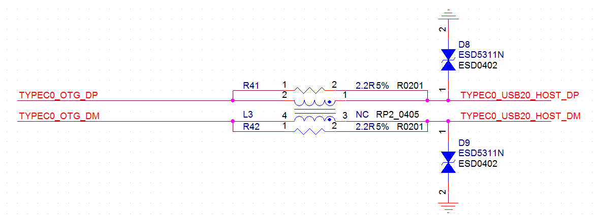
- The DM DP pin needs to be connected in series with a 2.2R resistor and add ESD devices. Prevent electrostatic damage.
- OTG devices use the ID pin in the plug to distinguish between A/B devices. The ID ground is referred to as A-Device, which acts as a USB Host. A-Device always provides power to the bus. The suspended ID is referred to as B-Device, which acts as a USB Device. The USB Host/USB Device role of the device can be switched through HNP (Host Exchange Protocol).
- The USB A-type interface can be directly suspended without using an ID signal. Type A interface can be configured via software to operate on HOST or DEVICE via USB.
Pin Number |
Pin Name |
Describe |
|---|---|---|
| B29 | TYPEC0_OTG_DP | USB 2.0 P-terminal |
| B30 | TYPEC0_OTG_DM | USB 2.0 N-terminal |
| B59 | TYPEC0_USB20_VBUSDET | USB 2.0 voltage detection |
| B58 | TYPEC0_OTG_ID | Identification |
¶ Debug port
- The system can be debugged using the UART interface. Note that the UART debugging interface level output from the core board is 1.8V. Normally, it is necessary to increase the level conversion chip to 3.3V.
- The default baud rate for the serial port is 115200.
Pin Number |
Pin Name |
Describe |
|---|---|---|
| B80 | UART2_RX_M0_1V8_DEBUG | uart2 rxd |
| B81 | UART2_TX_M0_1V8_DEBUG | uart2 txd |

[rs0102yh8.pdf](/cm5/rs0102yh8.pdf)
¶ Power on
- The CM5 board supports automatic power-on or button power-on.
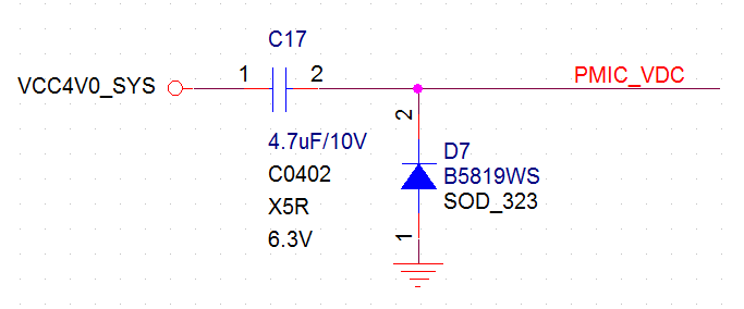
- CM5 B9 (PMIC_VDC): It is used to automatically start the external power supply. The recognized high level of the VDC pin is 0.8V, and it is recommended that the voltage be greater than 1V and less than or equal to 4V. When the VDC detects a high level, CM5 will turn on, and when the VDC is high, CM5 cannot be turned off (if an adapter is to be plugged in to turn on, it is necessary to set an RC delay for the VDC pin.
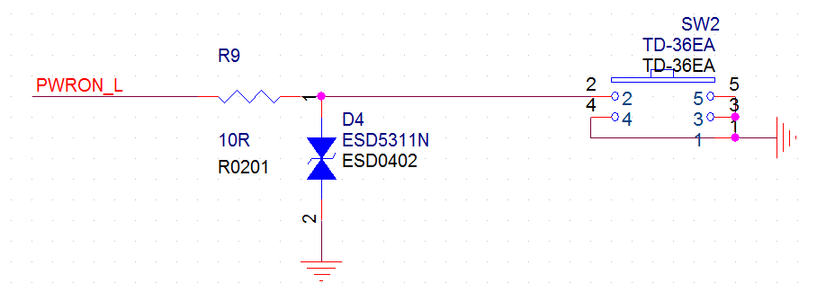
- CM5 A148 (PWRON_L): Connect the power on button, and there is a 45Kohm resistor inside the pin that is pulled up to VCC4V0_ On SYS, if the pin is pulled down for 20ms under shutdown status, it will be turned on. If the pin is pulled down for 20ms under startup status, it will cause short press/long press interrupts to the master controller. If the time is pulled down for more than 6s, it will be forced to turn off.
- General handling measures for keys include series resistance, adding ESD.
Pin Number |
Pin Name |
Describe |
|---|---|---|
| B9 | PMIC_VDC | power-on signal |
| A148 | PWRON_L | power signal |
¶ Usb interface
-
¶ USB TYPEC
- CM5 has two full-featured TYPEC interfaces, of which TYPEC0 can support USB OTG functionality, TYPEC1 only supports USB HOST functionality, and both TYPECs can support DP signal output.
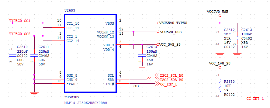
- In addition to the basic signal, the TYPEC interface design also requires a CC LOGIC detection chip for detecting different device inserts. Currently, the recommended chip model is FUSB302.
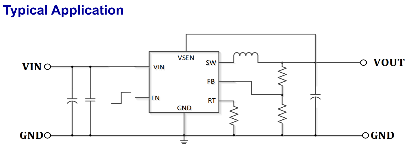
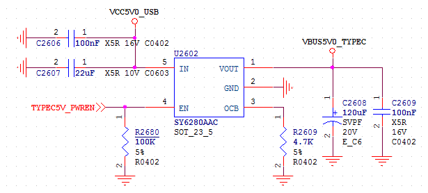
- In addition to the connector and FUSB302 chip, TYPEC also needs to add a load switch to the external output power supply, as shown in the following figure.
- The hardware connection methods of TYPEC1 and TYPEC0 are consistent.
Pin Number |
Pin Name |
Describe |
|---|---|---|
| B29 | TYPEC0_OTG_DP | usb20 dp |
| B30 | TYPEC0_OTG_DM | usb20 dm |
| B31 | TYPEC0_SSTX1P | dp tx1p |
| B32 | TYPEC0_SSTX1N | dp tx1n |
| B33 | TYPEC0_SSRX1P | dp tx0p |
| B34 | TYPEC0_SSRX1N | dp tx0n |
| B35 | TYPEC0_SSRX2P | dp tx2p |
| B36 | TYPEC0_SSRX2N | dp tx2n |
| B37 | TYPEC0_SSTX2P | dp tx3p |
| B38 | TYPEC0_SSTX2N | dp tx3n |
| B39 | TYPEC0_SBU1 | dp auxp |
| B40 | TYPEC0_SBU2 | dp auxn |
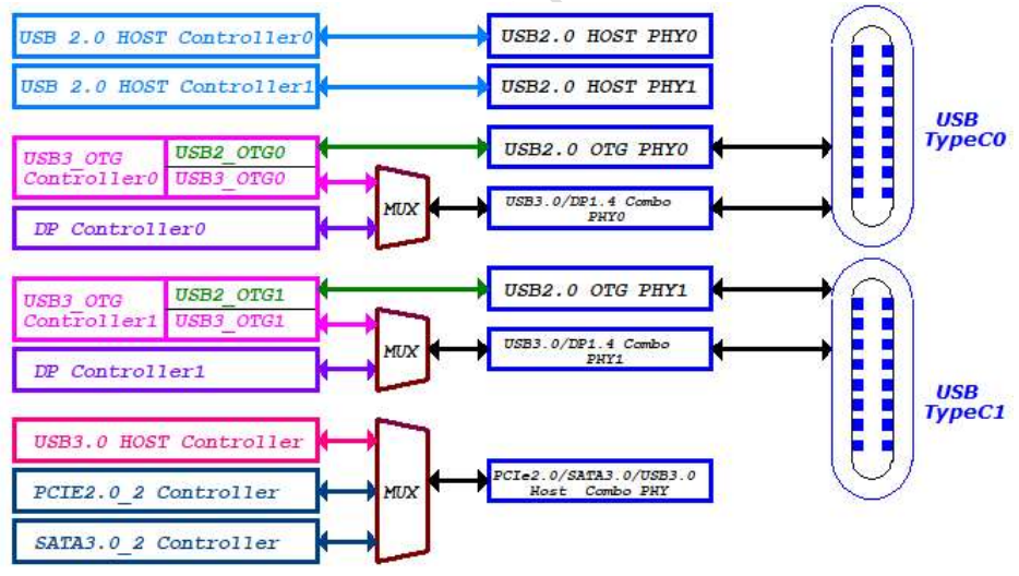
- Internal Reuse Relationship between USB PHY and USB Controller.
- The following figure shows the connection method of CC LOGIC detection chip.
- The connection method of the load switch can adjust the output current according to the requirements of the peripheral device.
- The Combo PHY of USB3.0/DP1.4 supports Lane to Lane switching (SWAP), so a TYPEC standard port can have the following five configurations:
- Type-C 4Lane(with DP function)

2. USB2.0 OTG+DP 4Lane(Swap OFF)

3. USB2.0 OTG+DP 4Lane(Swap ON)

4. USB3.0 OTG0+DP 2Lane(Swap OFF)

5. USB3.0 OTG+DP 2Lane(Swap ON)

-
¶ USB3.0
- The CM5 core board has three independent USB3.0 controllers, one of which can be used as an OTG interface, and the other two can only be used as HOST.
- The USB3.0 HOST controller has only a USB3.0 HOST and is not embedded with USB2.0. To form a complete USB3.0 HOST interface, it needs to be combined with USB2.0 HOST Controller1 (Configuration 1) or USB2.0 HOST Controller0 (Configuration 2) to form a standard USB3.0 HOST. The internal connection diagram is as follows:
- USB3.0 HOST2+USB2.0 HOST1

2. USB3.0 HOST2+USB2.0 HOST0

* The following table describes the PIN definitions for the USB3.0 OTG interface.
Pin Number |
Pin Name |
Describe |
|---|---|---|
| B29 | TYPEC0_OTG_DP | usb20 dp |
| B30 | TYPEC0_OTG_DM | usb20 dm |
| B35 | TYPEC0_SSRX2P | usb30 rxp |
| B36 | TYPEC0_SSRX2N | usb30 rxn |
| B37 | TYPEC0_SSTX2P | usb30 txp |
| B38 | TYPEC0_SSTX2N | usb30 txn |
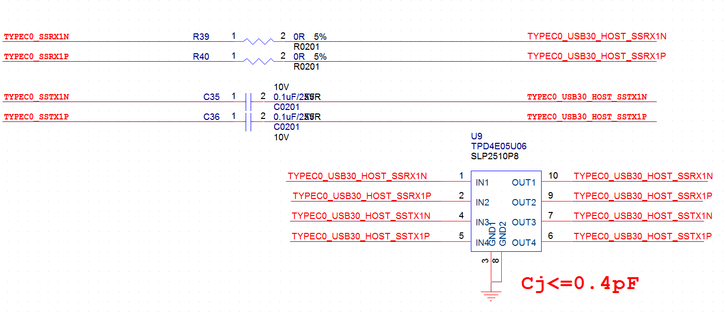
- Note that the RX end requires a series resistor and the TX end requires a series capacitor.
- The junction capacitance of ESD is less than 0.4pf, otherwise it will affect signal integrity.
* The following table describes the PIN definitions for the USB3.0 HOST1 interface.
Pin Number |
Pin Name |
Describe |
|---|---|---|
| B24 | TYPEC1_OTG_DP | usb20 dp |
| B25 | TYPEC1_OTG_DM | usb20 dm |
| B20 | TYPEC1_SSRX2P | usb30 rxp |
| B21 | TYPEC1_SSRX2N | usb30 rxn |
| B22 | TYPEC1_SSTX2P | usb30 txp |
| B23 | TYPEC1_SSTX2N | usb30 txn |
- The following table describes the PIN definitions for the USB3.0 HOST2 interface.
Pin Number |
Pin Name |
Describe |
|---|---|---|
| B11 | USB20_HOST0_DP | usb20 dp |
| B12 | USB20_HOST0_DM | usb20 dm |
| A102 | PCIE20_2_RXP | usb30 rxp |
| A103 | PCIE20_2_RXN | usb30 rxn |
| A104 | PCIE20_2_TXN | usb30 txp |
| A105 | PCIE20_2_TXP | usb30 txn |
-
¶ USB2.0
- The CM5 core board provides up to four sets of independent USB2.0 interfaces, of which one can be used as an OTG interface, and the other three can only be used as HOST. If there are many USB peripherals, HUB expansion can be added.
- TYPEC0_OTG_DP/DM is the system firmware writing port. If the product does not use this interface, it must be reserved during debugging and production, otherwise it will not be possible to debug and produce firmware writing.
- TYPEC0_ID There is approximately 200 Kohm resistor pulled up to USB20 inside the 1.8V.
- TYPEC0_USB20_VBUSDET is an OTG and Device mode detection pin that must be pulled out otherwise the USB device cannot be recognized when plugged into the computer.
Pin Number |
Pin Name |
Describe |
|---|---|---|
| B29 | TYPEC0_OTG_DP | usb20 dp |
| B30 | TYPEC0_OTG_DM | usb20 dm |
| B24 | TYPEC1_OTG_DP | usb20 dp |
| B25 | TYPEC1_OTG_DN | usb20 dm |
| B11 | USB20_HOST0_DP | usb20 dp |
| B12 | USB20_HOST0_DM | usb20 dm |
| B13 | USB20_HOST1_DP | usb20 dp |
| B14 | USB20_HOST1_DM | usb20 dm |
¶ Ethernet
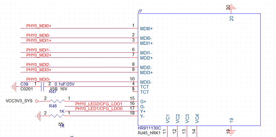
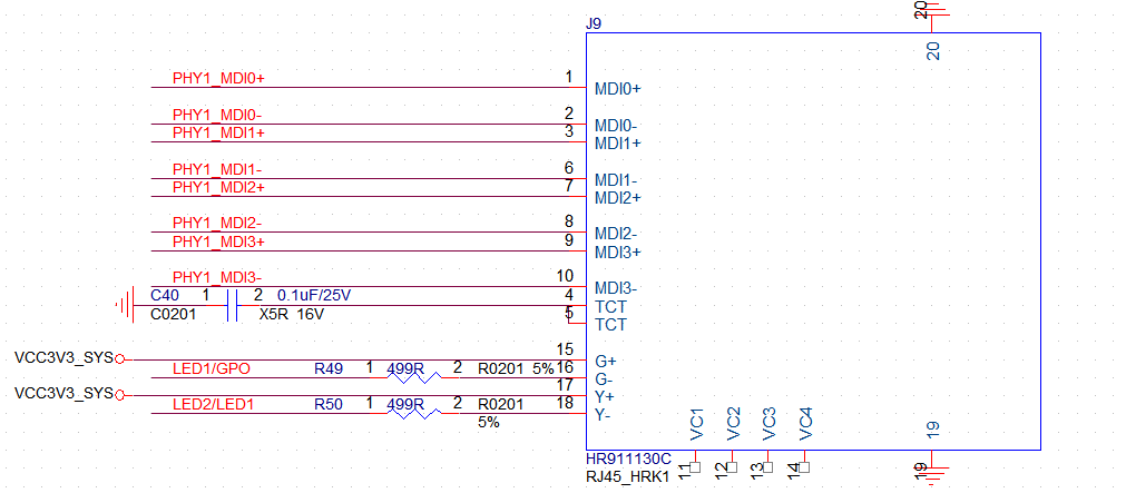
- The CM5 core board provides two gigabit Ethernet interfaces externally, with each interface having two independent LED control pins. Users only need to connect an external transformer and RJ45 socket to work.
- Note that the connection methods of the two PHY LEDs are different.
Pin Number |
Pin Name |
Describe |
|---|---|---|
| A33 | PHY0_LED1_LINK_L | PHY0_LED1_LINK_L |
| A34 | PHY0_LED2_ACT_H | PHY0_LED2_ACT_H |
| A35 | PHY0_MDI0+ | PHY0_MDI0+ |
| A36 | PHY0_MDI0- | PHY0_MDI0- |
| A37 | PHY0_MDI1+ | PHY0_MDI1+ |
| A38 | PHY0_MDI1- | PHY0_MDI1- |
| A39 | PHY0_MDI2+ | PHY0_MDI2+ |
| A40 | PHY0_MDI2- | PHY0_MDI2- |
| A41 | PHY0_MDI3+ | PHY0_MDI3+ |
| A42 | PHY0_MDI3- | PHY0_MDI3- |
Pin Number |
Pin Name |
Describe |
|---|---|---|
| B127 | PHY1_LED1_LINK_H | PHY1_LED1_LINK_H |
| B128 | PHY1_LED2_ACT_H | PHY1_LED2_ACT_H |
| B118 | PHY1_MDI3- | PHY1_MDI3- |
| B119 | PHY1_MDI3+ | PHY1_MDI3+ |
| B120 | PHY1_MDI2- | PHY1_MDI2- |
| B121 | PHY1_MDI2+ | PHY1_MDI2+ |
| B122 | PHY1_MDI1- | PHY1_MDI1- |
| B123 | PHY1_MDI1+ | PHY1_MDI1+ |
| B124 | PHY1_MDI0- | PHY1_MDI0- |
| B125 | PHY1_MDI0+ | PHY1_MDI0+ |
¶ Display interface
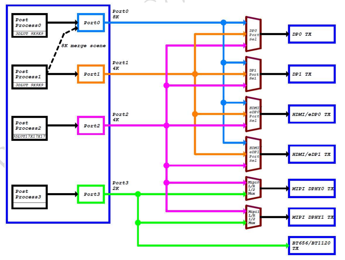
- The VOP controller of the RK3588 chip has four port outputs and supports DP0/DP1/HDMI0/eDP0/HDMI1/eDP1/MIPI DSI0/MIPI DSI1/BT656/BT1120 video interface output.
- A maximum of 4 standard screen displays are allowed, such as 4K+4K+4K+2K. If 8K needs to be supported, only 8K+4K+2K (where 8K is achieved by combining Post Process0 and Post Process1) is supported.
- The output path of RK3588 VOP and video interface is shown in the following figure:
-
¶ HDMI/eDP Combo PHY
- The CM5 core board has two HDMI/eDP TX Combo PHYs.
Pin Number |
Pin Name |
Describe |
|---|---|---|
| A2 | HDMI0_TX3N_PORT | HDMI0/eDP0_TX3N |
| A3 | HDMI0_TX3P_PORT | HDMI0/eDP0_TX3P |
| A4 | HDMI0_TX0N_PORT | HDMI0/eDP0_TX0N |
| A5 | HDMI0_TX0P_PORT | HDMI0/eDP0_TX0P |
| A6 | HDMI0_TX1N_PORT | HDMI0/eDP0_TX1N |
| A7 | HDMI0_TX1P_PORT | HDMI0/eDP0_TX1P |
| A8 | HDMI0_TX2N_PORT | HDMI0/eDP0_TX2N |
| A9 | HDMI0_TX2P_PORT | HDMI0/eDP0_TX2P |
| A10 | HDMI0_TX_SBDP | HDMI0_TX_SBDP/eDP0_AUXP |
| A11 | HDMI0_TX_SBDN | HDMI0_TX_SBDN/eDP0_AUXN |
- HDMI/eDP TX Combo PHY supports the following two modes:
- HDMI TX mode: maximum resolution support 8K@60Hz , supports RGB/YUV444/YUV420 (Up to 10bit) format.
- EDP TX mode: maximum resolution support 4K@60Hz , supports RGB/YUV422 (Up to 10bit) format.
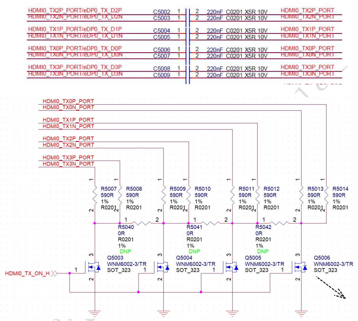
- The CM5 core board supports HDMI2.1 and downward HDMI2.0, while HDMI1.4 is compatible. As HDMI2.1 operates in FRL mode, when switching to HDMI2.0 or below mode, it operates in TMDS mode and should use an AC coupled voltage mode driver.
- As shown in the figure below, the capacitance value of AC coupling capacitors is 220nF and cannot be changed arbitrarily. It is recommended to use 0201 packaging for AC coupling capacitors, with lower ESR and ESL, which can also reduce impedance changes on the line.
-
¶ Display port
- The CM5 core board supports two DP1.4 TX PHYs (and USB3.0 Combo), with a maximum output resolution of up to 8K@30Hz.
- Each lane rate can support 1.62/2.7G/5.4/8.1Gbps.
- Supports 1Lane, 2Lane, or 4Lane modes.
- Supports RGB/YUV (Up to 10bit) format.
- Supports Single Stream Transport (SST).
- The usage and definition of DP1 and DP0 are consistent.
|Pin Number|Pin Name|Describe|
| :-: | :-: | :-: |
| B31 |TYPEC0_SSTX1P |dp tx1p |
| B32 |TYPEC0_SSTX1N |dp tx1n |
| B33 |TYPEC0_SSRX1P |dp tx0p |
| B34 |TYPEC0_SSRX1N |dp tx0n |
| B35 |TYPEC0_SSRX2P |dp tx2p |
| B36 |TYPEC0_SSRX2N |dp tx2n |
| B37 |TYPEC0_SSTX2P |dp tx3p |
| B38 |TYPEC0_SSTX2N |dp tx3n |
| B39 |TYPEC0_SBU1 |dp auxp |
| B40 |TYPEC0_SBU2 |dp auxn |
-
¶ Mipi tx d/cphy
- The CM5 core board has two MIPI D-PHY/C-PHY Combo PHY TX.
- D-PHY supports V2.0 version, with 0/1/2/3 lanes in D-PHY mode, with 2 wires per lane; Maximum transmission rate 4.5Gbps/Lane.
- C-PHY supports V1.1 version, with 0/1/2 Trio in C-PHY mode, and 3 wires per Trio A/B/C; Maximum transmission rate 5.7Gbps/Trio.
- The TX and RX of MIPI D-PHY/C-PHY Combo PHY0 can only be configured in DPHY0 TX and DPHY0 RX modes, or in both CPHY0 TX and CPHY0 RX modes. It does not support configuring one as DPHY0 TX and the other as CPHY0 RX.
- The TX and RX of MIPI D-PHY/C-PHY Combo PHY1 can only be configured in both DPHY1 TX and DPHY1 RX modes, or in both CPHY1 TX and CPHY1 RX modes. It does not support configuring one as DPHY1 TX and the other as CPHY1 RX.
- MIPI D/C-PHY0 operates in D-PHY mode,Supports x4Lane mode, MIPI_ DPHY0_ TX_ D [3:0] Data reference MIPI_ DPHY0_ TX_ CLK.
- MIPI D/C-PHY0 operates in C-PHY mode,Supports 0/1/2 Trio, with 3 wires per Trio A/B/C, MIPI_ CPHY0_ TX_ TRIO[2 : 0]_ A ,MIPI_ CPHY0_ TX_ TRIO[2:0]_ B, MIPI_ CPHY0_ TX_ TRIO[2:0]_ C.
- The support of MIPI D/C-PHY1 is consistent with PHY0.
¶ Camera interface
-
¶ Mipi rx d/cphy